How Does 5G Affect PCB Design and Manufacturing?

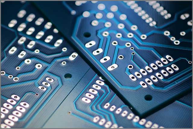
A Printed Circuit Board is the heart of simple and complex electronic devices. Hence, it is vital not only because it allows electrical connections between components but also because it carries analogue and digital signals, power supply lines, and data transmission signals.
But with the introduction of 5G, many new demands should be met when designing and manufacturing printed circuit boards. To help you understand more below is an outline of how 5G affects PCB design and manufacturing.
What is 5G?
5G is the fifth-generation technology available in various variations, including low-band, mid-band, and high-band variations. According to multiple studies, about 40 percent of the global population will utilize 5G networks by 2024.
Compared to 4G, 5G is faster, has a remarkable user experience, reduced latency, and enhanced reach for communications and Wi-Fi roaming.
Why is 5G essential for PCBs?
PCB manufacturers understand the impact of 5G on electronic devices. Hence, there is a need for significant manufacturing innovations to handle the demand.
Even though all sectors will feel the impact of 5G some years to come, the most significant effect will likely be on the PCB manufacturing industry. This is because PCBs are the hearts of all modern electronics.
Therefore, PCB designers and manufacturers have embraced 5G, which has affected every production process area. Some of the places where 5G is essential for circuit boards are:
*Industry applications – introduction of 5G has expanded many sectors, including health care, manufacturing, automotive, communication, and many other industries.
*Customer awareness – since most customers are aware of 5G, PCB designers and manufacturers must keep up with the demands.
*Data traffic – due to its high speed, reliability, and low latency, 5G has been embraced in almost all sectors. This demands that PCB manufacturers develop new strategies to ensure the boards maintain reliable performance.
How does 5G affect PCB design and manufacturing?
PCB manufacturers and designers have managed to keep up with the evolving of technology by implementing procedural, design, and production processes that grow with 5G technology.
Some of the ways 5G has affected PCB design and manufacturing include:
Smaller designs
Modern electronics such as wearable fitness devices, smartphones, and other smart gadgets are changing as manufacturers move with the latest technologies. On the other hand, printed circuit boards need to change. This is because traditional circuit boards are not flexible or are too rigid.
Since electronics are becoming more and more powerful, they require smaller and lighter PCBs. But the PCBs should be well manufactured not to compromise the performance. Therefore, PCB manufacturers need to develop new technology, such as laser drilling, precise CNC machining and so on.
Thinner traces
A lot of 5G devices need high-density interconnect PCBs since the traces are thinner. This helps in preventing loss of signal. Since old PCB processing methods, such as subtractive design, can create crossed tracks on the PCB, manufacturers need to develop new strategies.
Most manufacturers have solved the issue by using a semi-additive fabrication process to build straighter and more precise traces for great circuit density.
AOI (Advanced Automated Optical Inspection) Systems
AOI systems are used to inspect the circuit boards during the manufacturing process. They can detect, identify, and repair any errors in design and performance or by comparing the designs before mass production.
Unlike manual inspection, AOI reduces time and makes employee involvement more advanced. Thus, manufacturers must optimize their AOI processes to conserve resources and reduce production time.
Moreover, 5G is a technology that requires sophisticated AOI systems to identify and correct even the slightest misalignments.
Applications of 5G PCB
5G printed circuit boards have many applications in different sectors. Some of the popular applications of 5G PCBs are:
Smart homes
With 5G PCBs, connecting gadgets such as iPads and phones to smart devices in your home are possible. This is done through a wireless connection to monitor and control various activities at home. Moreover, the super-fast 5G enables people to watch live CCTV videos on their mobile phones.
High-speed cellular network
Due to high 5G speeds, communication is made better. This is because the higher the speed, the faster the communication is services such as calling and messaging. Moreover, higher speeds make calls and bulk text messaging quicker and without challenges.
Logistics
A mobile device made of 5G can be linked to a high-speed 5G network for logistics tracking. It is also great for managing and delivering shipments online through smartphones.
Entertainment
Due to the high speed of the 5G network, it is possible to watch your popular live shows without downtime. For instance, you can watch movies on Netflix on a 5G PCB mobile device without significant breakages. In addition, you can download movies and videos at an outstanding speed.
Medical sector
5G is remarkable when it comes to medical surgery. This is because it helps to show live videos when doctors are operating on a patient.
Final Word
5G has secured its space in the digital world. Due to its faster speed, reliability, and enhanced user experience, it has a lasting effect on PCB design and manufacturing. PCB designers and manufacturers are putting more effort into the latest technology and catching up with the technology.
Although there are various challenges that PCB designers and manufacturers face in 5G, they have managed to come up with strategies that help them produce well-functioning 5G PCBs. The boards meet all the requirements of the 5G network and utilize the opportunities offered by 5G.


